For clear, magnified images and quick, targeted analyses of elemental composition, SEM-EDS is the method of choice.
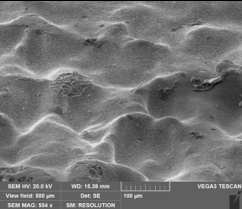
Introduction. A scanning electron microscope (SEM) can be used to examine samples at very high magnifications – up to 1 million times! The analysis of coating failures with an SEM typically only uses magnifications up to 10,000X, however, and most often magnifications attainable with a light microscope are used. An SEM has several other useful features that light microscopes lack. One of those features is its large depth of field that enables imaging of irregular surfaces without blurring. Images of the surface of a piece of steel obtained using an SEM are provided as Figures 1-6 below in order of increasing magnification. The coating on the steel had been removed using chemical stripper to expose the underlying steel surface for examination. Because of the depth of field, the entire image can be in focus simultaneously, whether at low or high magnification. The clarity of the images far surpasses what could be attained with a light microscope.
Analysis by SEM. An SEM scans a select area of a sample in a raster-like pattern with a focused beam of high energy electrons and analyzes the returning signal. Three different imaging modes can be used: secondary electrons (SE), backscattered electrons (BSE), and x-ray; each of which has its own detector.
Electrons that are dislodged from atoms located near the surface of the sample are termed “secondary electrons.” These electrons are attracted to the microscope’s positively charged SE detector, and the resulting electrical signal generated is translated into a gray-scale image, where the gradations of gray depict the 3D surface structure. The images represented in Figures 1-3 were generated in SE mode. SE mode probes a volume of sample near the surface, as shown in Figure 7, and, as a result, the images produced have the familiar look of a common photograph. SE emanating from deeper within the sample are absorbed by other atoms because SE are low energy.
Some of the electrons in the electron beam ricochet off atoms in the specimen. No energy is lost when the electron reflects, so the back-scattered electrons (BSE) remain high in energy and, as a result, can emanate from deeper within the sample than SE, as shown in Figure 7. Thus, the images produced in BSE mode do not reflect the topography of a sample as well as an SE image. Because the BSE are more likely to reflect off heavier atoms, the tones in the gray-scale image generated vary with atomic number, with heavier atoms appearing lighter in color and lighter atoms appearing darker. The images of a crack in the steel surface in Figures 4-6 were obtained through detection of BSE.


EDS. Energy-dispersive X-Ray Spectroscopy (EDS) is used in conjunction with SEM to identify the elemental composition near the surface of the sample. The detection limit is roughly 0.1% or 1000 ppm. When a secondary electron is dislodged from an atom, the resulting hole is filled by an electron from a higher energy level. The electron falling into the hole loses a characteristic amount of energy equal to the energy difference between the energy levels, and this energy is released in the form of an X-ray. The X-rays are higher in energy than the SE and BSE and therefore can emanate from deeper within the specimen, as illustrated in Figure 7.
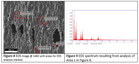
SE and BSE mode can be used to locate the area of interest for subsequent EDS analysis. The entire area of the image can be analyzed or smaller areas or even points in the image can be selected for analysis, as illustrated in Figure 8. A spectrum is generated for each area and point analyzed, and the spectra are analyzed to provide an indication of the relative amounts of the elements or trends in elemental composition. An example of an EDS spectrum is shown in Figure 9.
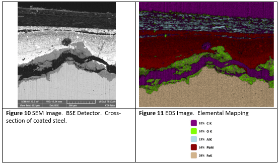
Figures 10 and 11 show images of a piece of steel from a bridge in Pittsburgh that was coated with three layers of paint over mill scale. The gradations of gray in the BSE image obtained with the SEM (Figure 10) are indicative of the location of the various elements present in the sample. The EDS image in Figure 11 shows a color-coded map of some of the elements identified. The purple areas are organic coatings, the red area is a lead-based paint, the green area is mill scale, and the tan area is the steel substrate.
Application of SEM-EDS for the Analysis of Coating Failures. Images obtained in SE mode depict the topography of the sample’s surfaces and can be used to examine the surface profile of the substrate or cross-section of a coating. The number of coating layers and their thicknesses can be determined, sometimes even when the coating layers are the same color. The BSE mode can be used to image variations in the elemental composition of localized areas of the sample and identify contaminants and inclusions, the elemental composition of which can then be determined using EDS. The chemical analysis performed by EDS is quick. After the areas or points on the image are selected, a qualitative analysis can be completed in approximately 30 seconds.
Limitations of EDS. When analyzing coating samples, EDS produces relatively good qualitative results, but not good quantitative results. The elemental composition is based on calculations that may not be accurate for many reasons. EDS is considered a semi-quantitative tool; that is, it is useful for determining relative concentrations of different elements and trends in composition. Other limitations:
- EDS is not able to detect hydrogen;
- The detection limit of 1000 ppm is relatively high; and
- Some elements appear in the spectrum at almost the same location as other elements and their peaks cannot be deconvoluted.


thank you for the information
muhammed…
You’re welcome! We’re glad it was helpful.